Discover Premium Ceramic Products | Durability & Elegance United | Advanced Ceramics
1. Introduction
Just yesterday, semiconductor giant TSMC announced a $4 billion expansion of its Arizona facility to address global chip shortages. This massive investment spotlights the extreme precision required in silicon crystal production – where silicon carbide crucibles play an indispensable role. These specialized containers form the heart of crystal growth furnaces, enabling the ultra-pure silicon wafers powering our smartphones, EVs, and AI infrastructure.

*(This caption directly identifies the material shown, connects it to the semiconductor manufacturing context of the surrounding text, and highlights its key functional benefit (thermal management) without unnecessary prefixes.)*
2. The Crucible’s Mission: Growing Perfect Crystals
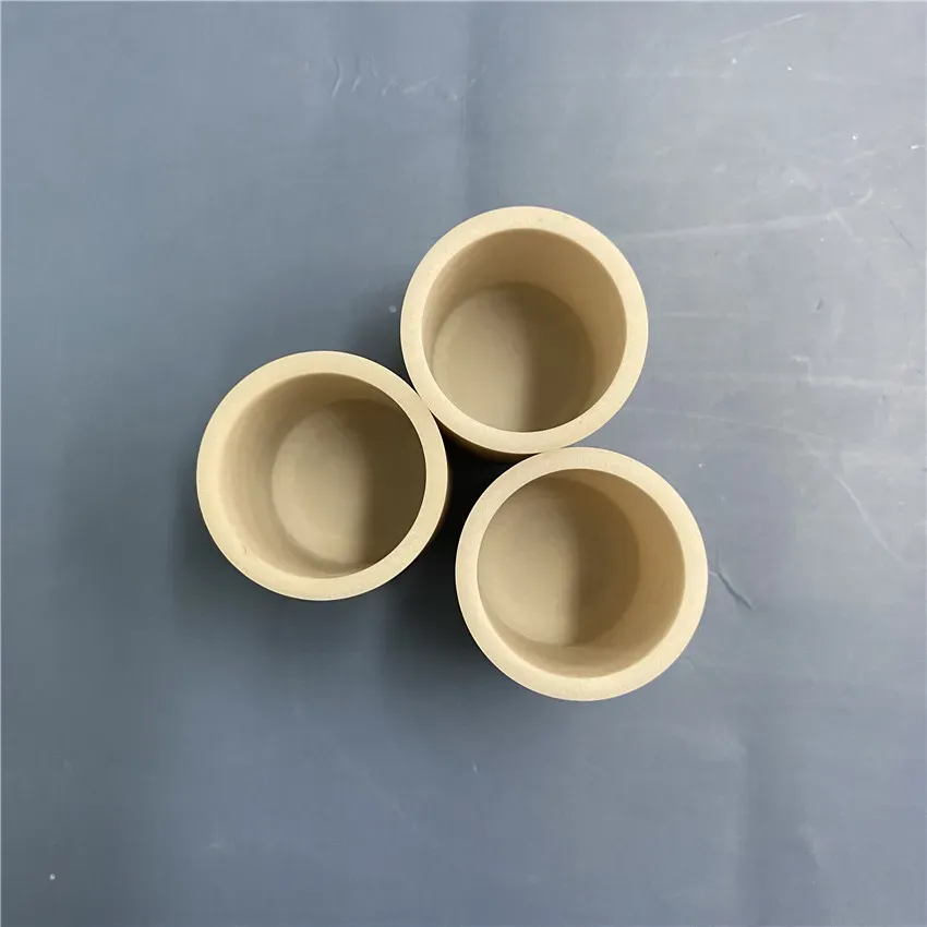
In the Czochralski process, polycrystalline silicon melts at 1,414°C inside a crucible. A seed crystal dips into this molten bath and slowly withdraws, forming a pristine single-crystal ingot. This demands a container that won’t contaminate the silicon or fail under brutal thermal cycling. That’s where silicon carbide crucibles shine.
Their secret lies in silicon carbide’s exceptional properties: thermal conductivity triple that of stainless steel, incredible hardness (second only to diamond), and near-zero thermal expansion. Crucibles made from recrystallized silicon carbide (RBSiC) maintain structural integrity through hundreds of cycles, unlike cheaper quartz alternatives that degrade rapidly.
3. Why Silicon Carbide Dominates Semiconductor Furnaces
When selecting crucible materials, engineers compare key performance indicators. Let’s examine how silicon carbide stacks up against common alternatives:

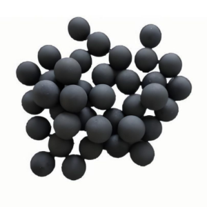
- Boron carbide vs silicon carbide: While boron carbide offers superior neutron absorption, silicon carbide provides better thermal shock resistance and cost-effectiveness for crystal growth.
- Silicon nitride crucibles: Though silicon nitride ceramic offers excellent fracture toughness, silicon carbide crucibles maintain higher thermal conductivity (120 W/mK vs 30 W/mK) – crucial for uniform temperature distribution.
Silicon carbide crucibles achieve contamination levels below 1 ppm. This purity prevents doping defects in wafers, directly impacting chip yields. Recent advances in chemical vapor deposition (CVD) coatings further enhance their lifespan in corrosive molten silicon environments.
4. Supporting Cast: Silicon Carbide Components in Crystal Growth
Beyond crucibles, semiconductor furnaces incorporate numerous silicon carbide elements:
- Silicon carbide tubes and silicon carbide mullite tubes serve as thermocouple protection sleeves and furnace liners
- Silicon carbide burner nozzles ensure precise gas injection
- Silicon nitride plates and custom silicon nitride heat shields guard sensitive components
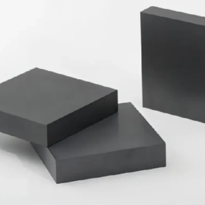
- RBSiC silicon carbide tile blocks form furnace hearths
These components create the stable, contaminant-free environment required for growing 300mm crystal ingots – the current industry standard.
5. Beyond Semiconductors: Unexpected Silicon Carbide Applications
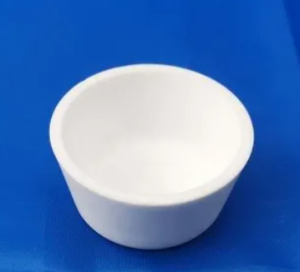
Interestingly, the same material properties valuable in furnaces make silicon carbide ceramics popular in kitchens:
- Silicon carbide ceramic baking dishes and casserole dishes distribute heat evenly
- Silicon carbide ceramic dinner plates withstand thermal shock from oven to table
- Specialized forms like silicon carbide ceramic pie dishes and ramekins are gaining chef endorsements
Luxury brands like Staub even market silicon carbide baking dish lines. While these culinary items use different manufacturing techniques, they share the core material advantages exploited in industrial settings.
6. Future Frontiers and Material Innovations
As chipmakers push for larger 450mm wafers, crucible manufacturers respond with innovations:
- Porous silicon carbide ceramic tubes for advanced gas diffusion
- Silicon carbide diamond grinding discs for precision machining
- High-purity silicon nitride powder market growth for hybrid components
Ongoing research into silicon carbide piezoelectric ceramic discs may even enable integrated process monitoring in next-gen crucibles.
7. Conclusion
From enabling the smartphone in your pocket to the casserole in your oven, silicon carbide ceramics demonstrate remarkable versatility. In semiconductor manufacturing specifically, silicon carbide crucibles remain irreplaceable for growing the perfect crystals underpinning our digital world. As chip geometries shrink and wafer sizes increase, these unassuming containers will continue playing a starring role in technological progress.
Discover the KINTEK SOLUTION Advantage: Elevate your semiconductor manufacturing with our premium silicon carbide crucibles. Engineered for unparalleled purity and thermal performance, our crucibles are the cornerstone of crystal growth perfection. Don’t compromise on quality – let KINTEK SOLUTION be your trusted partner. Contact us today to explore how our cutting-edge solutions can transform your process!
RELATED POSTS
Pioneering Boron Nitride vs. Silicon Carbide Ceramics: Unveiling Game-Changing Innovations for Global Procurement Excellence
Why Are Silicon Carbide Crucibles Essential in High-Temperature Crystal Growth?
Unlock the Power of Silicon Carbide Crucibles in High-Temperature Semiconductor Manufacturing
Differences and Applications Between Ceramic and Metal Crucibles