Discover Premium Ceramic Products | Durability & Elegance United | Advanced Ceramics
1. Introduction
In a major development reported just hours ago, leading semiconductor materials supplier Wolfspeed announced a breakthrough in 200mm silicon carbide (SiC) wafer production, citing enhanced crystal quality achieved through the use of proprietary silicon carbide crucibles in their physical vapor transport (PVT) furnaces. This milestone underscores a growing industry shift toward SiC-based containment solutions for high-fidelity crystal growth—a niche but mission-critical application where material purity and thermal resilience are non-negotiable.
While silicon carbide is widely recognized for industrial abrasives, armor plating (e.g., silicon carbide ceramic tiles), and even kitchenware like silicon carbide ceramic baking dishes, its role as a crucible material in advanced semiconductor manufacturing represents one of its most demanding and sophisticated uses. Unlike conventional graphite or quartz crucibles, silicon carbide crucibles offer unparalleled resistance to chemical erosion and thermal shock at temperatures exceeding 2,200°C—conditions essential for growing single-crystal SiC ingots.
2. Why Silicon Carbide Crucibles Are Indispensable in Crystal Growth
The production of high-quality silicon carbide wafers begins with sublimation-based crystal growth inside sealed, high-temperature furnaces. During this process, raw SiC powder is heated until it sublimates, then re-deposits as a monocrystalline boule on a seed crystal. Any contamination from the crucible can introduce defects that compromise electrical performance.
Silicon carbide crucibles mitigate this risk because they are chemically compatible with the SiC vapor environment. Unlike boron carbide vs silicon carbide comparisons in armor applications—where hardness and density dominate—here, vapor-phase compatibility is paramount. Boron carbide would decompose and contaminate the melt, while traditional ceramics like alumina react aggressively with silicon vapors.
Moreover, silicon carbide exhibits exceptional thermal conductivity (up to 120 W/m·K), enabling uniform temperature distribution across the crucible walls. This minimizes thermal gradients that cause dislocations in the growing crystal—a key factor in yield improvement for power device manufacturers.
3. Performance Advantages Over Alternatives Like Silicon Nitride

Some manufacturers have explored silicon nitride crucible factory offerings as potential alternatives due to silicon nitride’s high strength and oxidation resistance. However, silicon nitride begins to degrade above 1,800°C in inert atmospheres and can release nitrogen into the SiC vapor phase, altering stoichiometry and doping profiles.
In contrast, silicon carbide remains stable well beyond 2,400°C under argon or vacuum. Components such as custom silicon nitride heat shields or silicon nitride rings may be used elsewhere in the furnace assembly, but the crucible itself demands the superior refractoriness of SiC. Even high purity silicon nitride powder market advancements haven’t closed this performance gap for direct melt contact.
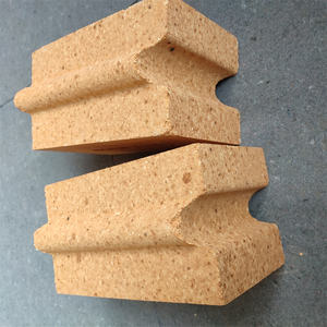
Additionally, structural forms like rbsic silicon carbide tile blocks or silicon carbide ceramic columns are engineered for furnace linings, but only monolithic or sintered silicon carbide crucibles provide the seamless, non-porous interior required to prevent particle shedding during crystal growth.
4. Supporting Infrastructure: Tubes, Discs, and Precision Components
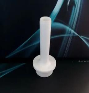
Beyond the crucible itself, the entire PVT system relies on complementary silicon carbide components. Silicon carbide thermocouple protection tubes shield sensors from corrosive vapors while maintaining rapid thermal response. Silicon carbide ceramic tubes for high-temperature zones ensure gas flow integrity without outgassing.
Precision elements like silicon carbide rings and silicon carbide discs serve as sealing and alignment fixtures, leveraging the material’s dimensional stability. Even silicon carbide ceramic disc taps or grinding discs used in post-processing benefit from the same base material science—though these serve entirely different functions than crucibles.
Notably, consumer-grade items such as silicon carbide ceramic dinner plates or silicon carbide baking dish staub products share the base compound but lack the ultra-high purity (>99.99%) and controlled microstructure essential for semiconductor applications. The crucible-grade material undergoes rigorous sintering protocols absent in tableware manufacturing.
5. Future Outlook and Industrial Scaling
As demand surges for electric vehicle inverters and 5G RF amplifiers, the need for larger, defect-free SiC wafers intensifies. Companies are now investing in 150mm and 200mm boule growth, which requires correspondingly larger silicon carbide crucibles with even tighter tolerances. Innovations in binder-free sintering and additive manufacturing of SiC components may soon enable complex geometries that further optimize vapor transport dynamics.
Meanwhile, hybrid systems incorporating silicon carbide porous ceramic tubes for gas injection or silicon carbide mullite tube composites for thermal zoning are under development. These advances reinforce silicon carbide’s dominance not just as a crucible material, but as the backbone of the entire high-temperature semiconductor crystal growth ecosystem.
6. Conclusion
The silicon carbide crucible exemplifies how a specialized ceramic component can enable transformative technologies. Far removed from everyday items like silicon carbide ceramic salad bowls or silicon carbide blue white porcelain plates, its role in semiconductor manufacturing demands extreme purity, thermal resilience, and chemical inertness. As the industry pushes toward larger wafers and higher yields, the silicon carbide crucible will remain an irreplaceable enabler of the next generation of power electronics.
Our Website founded on October 17, 2012, is a high-tech enterprise committed to the research and development, production, processing, sales and technical services of ceramic relative materials such as Silicon. Our products includes but not limited to Boron Carbide Ceramic Products, Boron Nitride Ceramic Products, Silicon Carbide Ceramic Products, Silicon Nitride Ceramic Products, Zirconium Dioxide Ceramic Products, etc. If you are interested, please feel free to contact us.