Discover Premium Ceramic Products | Durability & Elegance United | Advanced Ceramics
1. Introduction
When you think of cutting-edge tech—smartphones, electric vehicles, or AI chips—you probably don’t picture a humble crucible. Yet behind every high-performance semiconductor lies a silent workhorse: the silicon carbide crucible. Unlike the more familiar kitchenware like silicon carbide ceramic baking dishes or dinner plates, industrial silicon carbide crucibles operate in extreme conditions where purity, stability, and durability are non-negotiable.

These crucibles aren’t just containers—they’re enablers of precision. In this article, we’ll dive into one of their most demanding applications: crystal growth for semiconductors. We’ll also compare silicon carbide with related materials like boron carbide and silicon nitride, and explain why this ceramic reigns supreme in high-temperature processing.
2. Why Silicon Carbide Crucibles Excel in Crystal Growth
2.1. The Demands of Semiconductor Crystal Production
Growing single-crystal ingots—like monocrystalline silicon or gallium arsenide—requires melting raw materials at temperatures exceeding 1,400°C (2,550°F) in an ultra-clean environment. Any contamination from the crucible can ruin the entire batch, leading to defective chips or reduced yields. This is where silicon carbide crucibles shine.
Silicon carbide (SiC) offers exceptional thermal conductivity, low thermal expansion, and outstanding chemical inertness. It resists reaction with molten silicon and other semiconductor materials, minimizing impurity diffusion. Plus, its high mechanical strength prevents deformation during prolonged high-temperature exposure.
2.2. Silicon Carbide vs. Boron Carbide vs. Silicon Nitride

Engineers sometimes consider alternatives like boron carbide or silicon nitride for high-temp applications. But each has trade-offs.
- Boron carbide vs silicon carbide: While boron carbide is harder, it’s more brittle and can introduce boron impurities into silicon melts—disastrous for semiconductor doping control.
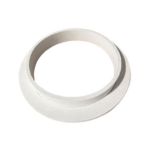
- Silicon nitride crucible factory output often focuses on components like silicon nitride rings or custom silicon nitride heat shields, which excel in oxidation resistance but lack the thermal conductivity of SiC. Silicon nitride plates and high purity silicon nitride powder market products are better suited for structural supports than direct melt contact.
In contrast, silicon carbide crucibles maintain structural integrity while enabling efficient heat transfer—critical for controlled solidification during crystal pulling (Czochralski or Bridgman methods).
3. Real-World Application: Growing Silicon Ingots for Solar and Chips
One of the most widespread uses of silicon carbide crucibles is in directional solidification furnaces for multicrystalline silicon ingots used in solar panels. Here, large silicon carbide crucibles—sometimes lined with specialized coatings—hold hundreds of kilograms of molten silicon.
The crucible must withstand thermal cycling, resist wetting by molten silicon, and not shed particles. Silicon carbide ceramic tubes and silicon carbide thermocouple protection tubes are often integrated into the same furnace setup, creating a fully SiC-compatible thermal environment.
For higher-purity applications like power electronics, monocrystalline silicon is grown using Czochralski furnaces. Though quartz crucibles are common here, advanced systems increasingly use coated or composite silicon carbide crucibles to extend service life and reduce oxygen contamination.
4. Supporting Components: Beyond the Crucible
The ecosystem around silicon carbide crucibles includes a range of specialized parts—all leveraging SiC’s robustness:
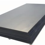
- Silicon carbide ceramic columns and silicon carbide brick line furnace interiors for insulation and support.
- Silicon carbide burner nozzles ensure clean, high-temp combustion in heating zones.
- RBSiC (reaction-bonded silicon carbide) silicon carbide tile blocks provide wear-resistant flooring or shielding in processing areas.
Even silicon carbide discs—such as silicon carbide ceramic grinding discs or silicon carbide diamond grinding discs for pottery—are used in post-processing to shape or polish grown crystals, though in semiconductor fabs, diamond-coated tools dominate.
5. Why Not Use Silicon Carbide Dinnerware in the Lab?
It’s tempting to draw parallels between industrial and consumer SiC products—like silicon carbide ceramic dinner plates or silicon carbide ceramic casserole dishes—but the similarity ends at the base material. Kitchenware uses lower-purity, often glazed SiC for aesthetics and thermal shock resistance, not ultra-high purity.
A silicon carbide baking ceramic dish from Staub or a silicon carbide ceramic butter dish with lid is engineered for oven-to-table use, not 1,600°C melts. Industrial crucibles are sintered or reaction-bonded to near-theoretical density with tightly controlled grain structure—far beyond what’s needed for a casserole.
6. Conclusion
In the high-stakes world of semiconductor manufacturing, the silicon carbide crucible is far more than a container—it’s a precision enabler. Its unmatched blend of thermal stability, chemical resistance, and mechanical strength makes it indispensable for growing the ultra-pure crystals that power modern electronics. While materials like silicon nitride and boron carbide have their niches, silicon carbide remains the gold standard for direct melt contact in extreme environments. As chipmakers push toward smaller nodes and wider bandgap semiconductors like SiC itself, demand for high-performance silicon carbide crucibles will only grow.
Our Website founded on October 17, 2012, is a high-tech enterprise committed to the research and development, production, processing, sales and technical services of ceramic relative materials such as Silicon. Our products includes but not limited to Boron Carbide Ceramic Products, Boron Nitride Ceramic Products, Silicon Carbide Ceramic Products, Silicon Nitride Ceramic Products, Zirconium Dioxide Ceramic Products, etc. If you are interested, please feel free to contact us.
RELATED POSTS
How to Properly Use and Maintain a Silicon Carbide Crucible for High-Temperature Applications?
What Makes Silicon Carbide Crucibles Essential in High-Temperature Industrial Applications?
Silicon Carbide Crucibles Are Quietly Powering the Future of Space-Grade Crystal Growth
How to Properly Use and Maintain a Silicon Carbide Crucible: A Step-by-Step Guide
7 Sizzling Facts About Silicon Carbide Crucibles (and Why Your Kitchen Might Secretly Want One)