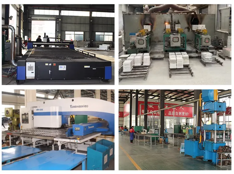
Discover Premium Ceramic Products | Durability & Elegance United | Advanced Ceramics
1. Introduction
Just 24 hours ago, Wolfspeed announced a major breakthrough in its Durham, North Carolina facility: the successful ramp-up of 200mm silicon carbide wafer production using proprietary crystal growth furnaces lined with ultra-stable silicon carbide crucibles. This milestone underscores a quiet but vital truth—the future of electric vehicles, 5G infrastructure, and grid-scale renewables hinges not just on chip design, but on the humble crucible that withstands temperatures above 2,200°C without contaminating the melt.

While many associate silicon carbide with armor or abrasives, its most demanding application lies in semiconductor manufacturing—specifically in the physical vapor transport (PVT) method used to grow bulk SiC crystals. Here, the silicon carbide crucible isn’t just a container; it’s an engineered component that directly influences crystal quality, yield, and scalability.
2. Why Silicon Carbide Crucibles? The Physics of Purity and Stability
2.1. The Extreme Environment of SiC Crystal Growth
Growing a single-crystal ingot of silicon carbide requires sublimating high-purity SiC powder at around 2,300°C in an inert atmosphere. At these temperatures, most ceramics react, deform, or leach impurities. Alumina crucibles crack. Graphite crucibles introduce carbon contamination. Even boron carbide vs silicon carbide comparisons show boron’s volatility makes it unsuitable for high-purity semiconductor applications.
Silicon carbide crucibles, however, offer near-perfect chemical inertness, exceptional thermal conductivity, and minimal thermal expansion. These properties prevent crucible failure during rapid heating cycles and ensure the vaporized SiC recondenses as a defect-free monocrystal—not a polycrystalline mess.

2.2. Material Purity Matters
Not all silicon carbide crucibles are equal. Industrial-grade versions may contain sintering aids like aluminum or boron that outgas at high temps. For semiconductor use, crucibles must be made from high-purity silicon carbide (>99.99%) with controlled grain structure. This is where manufacturers differentiate themselves—through proprietary forming and sintering techniques that eliminate microcracks and impurities.
3. Beyond the Crucible: Integrated High-Temp Components
3.1. Supporting Architecture in the Growth Chamber

The crucible doesn’t work alone. It’s part of a precision ecosystem inside the PVT furnace:
- Silicon carbide ceramic tubes shield thermocouples and provide gas flow channels.
- Silicon carbide rings act as spacers and thermal stabilizers.
- Silicon carbide burner nozzles regulate inert gas injection without eroding.
- RBSiC (reaction-bonded silicon carbide) silicon carbide tile blocks line furnace walls for uniform heat distribution.
These components—often custom-machined from dense silicon carbide ceramic columns or bricks—must match the crucible’s thermal behavior to avoid stress fractures.
3.2. Silicon Nitride: A Complementary Player
In some advanced setups, silicon nitride ceramic parts appear alongside silicon carbide. While silicon nitride crucible factories exist, pure silicon nitride lacks the thermal conductivity needed for the main crucible. However, custom silicon nitride heat shields, silicon nitride plates, and silicon nitride rings are used in cooler zones for their excellent shock resistance and electrical insulation.
The high purity silicon nitride powder market is growing, but for crystal growth, silicon carbide remains irreplaceable at the core.
4. Real-World Impact: From Lab to EV Charger
Each 150mm SiC boule grown in a silicon carbide crucible can yield hundreds of power devices. These chips switch electricity more efficiently than silicon, reducing energy loss in everything from Tesla inverters to solar microinverters. Without reliable, reusable silicon carbide crucibles, scaling production would be impossible—and costs would remain prohibitive.
Manufacturers now iterate crucible designs weekly, optimizing wall thickness, internal geometry, and surface finish to boost crystal growth rates by 15–20% per generation. Some even embed silicon carbide discs as baffles to control vapor flow dynamics.
5. Conclusion
The silicon carbide crucible may never grace a dinner table like silicon carbide ceramic dinner plates or a silicon carbide baking dish Staub—but in the silent, superheated heart of a crystal growth furnace, it’s enabling the clean energy revolution. As demand for wide-bandgap semiconductors surges, this niche ceramic component will only grow more critical, proving that sometimes, the most advanced technology starts in the simplest vessel.
Our Website founded on October 17, 2012, is a high-tech enterprise committed to the research and development, production, processing, sales and technical services of ceramic relative materials such as Silicon. Our products includes but not limited to Boron Carbide Ceramic Products, Boron Nitride Ceramic Products, Silicon Carbide Ceramic Products, Silicon Nitride Ceramic Products, Zirconium Dioxide Ceramic Products, etc. If you are interested, please feel free to contact us.
