Discover Premium Ceramic Products | Durability & Elegance United | Advanced Ceramics
1. Introduction
Just 24 hours ago, leading semiconductor materials supplier Wolfspeed announced a major expansion of its silicon carbide wafer production facility in Germany—citing unprecedented demand for electric vehicle (EV) power modules. Central to this scaling effort? The humble yet indispensable silicon carbide crucible, which enables the high-purity crystal growth essential for next-gen chips.

While most people associate silicon carbide with armor plating or brake discs, its role in advanced manufacturing—especially semiconductor fabrication—is quietly revolutionizing clean energy tech. In this article, we’ll zoom in on one hyper-specialized application: using silicon carbide crucibles for growing single-crystal silicon ingots under extreme thermal and chemical conditions.
2. Why Silicon Carbide Crucibles? The Science Behind the Choice
2.1. Thermal Stability at Extreme Temperatures
Silicon melts at around 1,414°C, but industrial crystal growth often pushes beyond 1,600°C. At these temperatures, conventional ceramics crack or react with molten silicon. Silicon carbide crucibles, however, maintain structural integrity up to 1,800°C in inert atmospheres—thanks to their covalent bonding and low thermal expansion.
2.2. Chemical Inertness and Purity
Impurities as small as parts per billion can ruin semiconductor performance. Silicon carbide crucibles offer exceptional resistance to molten silicon and dopant gases (like boron or phosphorus), minimizing contamination. This is where they clearly outperform boron carbide vs silicon carbide comparisons—boron carbide can leach boron into the melt, unintentionally doping the crystal.
3. Real-World Application: Czochralski and Directional Solidification Processes
In the Czochralski (CZ) method, a seed crystal is dipped into molten silicon and slowly pulled upward to form a monocrystalline ingot. The crucible must not only withstand heat but also resist erosion from convection currents and reactive gases.
Similarly, in directional solidification used for silicon wafers in solar cells, silicon carbide crucibles line the furnace chamber. Their thermal conductivity ensures uniform cooling—a key factor in reducing defects.
4. Beyond the Crucible: Complementary Silicon Carbide Components
A full high-temperature crystal growth system relies on more than just the crucible. Engineers often integrate:
- silicon carbide ceramic columns for structural support
- silicon carbide ring components for alignment
- silicon carbide burner nozzles for precise flame control
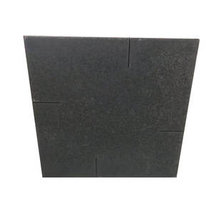
- rbsic silicon carbide tile blocks for furnace lining
- silicon carbide thermocouple protection tubes for accurate temperature monitoring
These parts work in concert to create a contamination-free, thermally stable environment—something traditional refractories simply can’t match.
5. Silicon Nitride: A Competitor or Complement?
Some might wonder about silicon nitride crucible factory offerings. While silicon nitride ceramic boasts excellent thermal shock resistance and is used in aerospace and bearings, it’s less stable in direct contact with molten silicon above 1,500°C. Silicon nitride can decompose, releasing nitrogen that contaminates the melt.
That said, custom silicon nitride heat shield components are sometimes used *around* the crucible—not in direct contact—to insulate sensitive zones. But for the crucible itself, silicon carbide remains unmatched.
6. Manufacturing Challenges and Innovations
Producing a high-purity silicon carbide crucible isn’t trivial. It requires sintering ultra-fine silicon carbide powder under controlled atmospheres to avoid oxide inclusions. Even minor porosity can trap impurities.
Recent advances include reaction-bonded silicon carbide (RBSC) techniques that yield near-net-shape crucibles with minimal machining—reducing cost and lead time for fabs racing to meet EV and 5G demands.
7. Not Just for Semiconductors: A Note on Other Uses
While this article focuses on crystal growth, it’s worth noting that silicon carbide’s versatility spans many forms—from silicon carbide ceramic baking dish products (marketed for even heating) to silicon carbide ceramic pipes used in corrosive chemical handling. However, these consumer or industrial uses don’t require the same purity standards as semiconductor crucibles.
Items like silicon carbide ceramic dinner plates or silicon carbide blue white porcelain plates leverage aesthetic and thermal properties—but lack the engineered microstructure needed for molten silicon containment.
8. Conclusion
As the world shifts toward electrification and renewable energy, the unsung hero enabling faster, more efficient power electronics may very well be the silicon carbide crucible. Its unique blend of thermal resilience, chemical inertness, and manufacturability makes it irreplaceable in cutting-edge semiconductor production. With companies like Wolfspeed scaling up, demand for these specialized components—and the expertise to produce them—will only grow.
Our Website founded on October 17, 2012, is a high-tech enterprise committed to the research and development, production, processing, sales and technical services of ceramic relative materials such as Silicon. Our products includes but not limited to Boron Carbide Ceramic Products, Boron Nitride Ceramic Products, Silicon Carbide Ceramic Products, Silicon Nitride Ceramic Products, Zirconium Dioxide Ceramic Products, etc. If you are interested, please feel free to contact us.