Discover Premium Ceramic Products | Durability & Elegance United | Advanced Ceramics
1. Introduction
Just 24 hours ago, Wolfspeed announced a major expansion of its silicon carbide wafer production facility in Germany, citing unprecedented demand from EV makers like BMW and Volkswagen. This news underscores a quiet but pivotal shift in semiconductor manufacturing: the move from traditional silicon to wide-bandgap materials like silicon carbide (SiC). At the heart of this transition lies a seemingly simple but technologically sophisticated component—the silicon carbide crucible.
While most consumers associate silicon carbide with ceramic dinnerware or sanding discs, its industrial-grade form is enabling breakthroughs in high-power electronics. In this article, we’ll dive into how the silicon carbide crucible has become indispensable in growing high-purity SiC crystals—a process that demands extreme temperatures, chemical inertness, and dimensional stability.
2. Why Silicon Carbide Crucibles? The Physics of Crystal Growth
2.1. The PVT Process and Crucible Requirements
Silicon carbide wafers are primarily grown using the Physical Vapor Transport (PVT) method, which involves heating high-purity SiC powder to over 2,200°C in a sealed chamber. At these temperatures, the powder sublimates and re-deposits as a single crystal on a seed substrate. The crucible holding the source material must withstand this extreme environment without contaminating the melt or deforming.
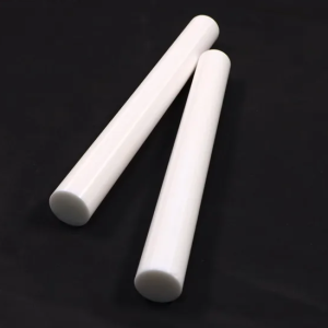
Graphite crucibles were historically used, but they introduce carbon impurities and degrade rapidly. Enter the silicon carbide crucible: made from sintered or reaction-bonded SiC (often labeled as RBSiC silicon carbide tile block in industrial catalogs), it offers superior thermal conductivity, minimal thermal expansion, and exceptional resistance to chemical attack—even in reducing atmospheres.
2.2. Purity Matters: High-Purity vs. Standard Grades
Not all silicon carbide crucibles are created equal. For semiconductor applications, manufacturers require ultra-high-purity variants with impurity levels below 10 ppm. These crucibles are distinct from those used in metallurgy or even from consumer items like silicon carbide ceramic baking dishes or silicon carbide ceramic dinner plates, which prioritize aesthetics and food safety over atomic-level cleanliness.
3. Material Showdown: Boron Carbide vs Silicon Carbide and Beyond
When evaluating high-temperature ceramics, engineers often compare boron carbide vs silicon carbide. Boron carbide is harder and lighter, but it oxidizes more readily above 800°C and is far more expensive. Silicon carbide, by contrast, maintains structural integrity up to 1,600°C in air and beyond 2,000°C in inert atmospheres—making it ideal for crucibles.
Some might wonder about silicon nitride as an alternative. While silicon nitride ceramic components—like silicon nitride rings, plates, or custom silicon nitride heat shields—are excellent for thermal shock resistance, they lack the thermal conductivity needed for uniform heat distribution in PVT systems. Plus, sourcing from a silicon nitride crucible factory doesn’t guarantee compatibility with SiC sublimation chemistry.
4. The Ecosystem of High-Temperature SiC Components

The silicon carbide crucible rarely works alone. It’s part of a broader suite of SiC-based furnace hardware designed for extreme conditions. These include:
- Silicon carbide ceramic tubes for furnace insulation and gas flow
- Silicon carbide thermocouple protection tubes
- Silicon carbide burner nozzles for precise heating
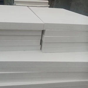
- Silicon carbide brick and silicon carbide ceramic columns for structural support
- Silicon carbide ring and silicon carbide discs for sealing and rotation mechanisms
Even silicon carbide ceramic piping and porous ceramic tubes find roles in gas handling and filtration within the same production lines. This integrated approach ensures minimal contamination and maximum process efficiency.
5. Beyond Semiconductors: Niche Cross-Applications
Interestingly, the manufacturing techniques developed for high-purity silicon carbide crucibles have trickled down into other sectors. For example, the same sintering processes yield durable silicon carbide ceramic serving bowls or silicon carbide ceramic casserole dishes with lids—though these are made from food-grade, not semiconductor-grade, material.
Similarly, silicon carbide ceramic disc taps and silicon carbide grinding discs benefit from the material’s hardness and wear resistance. However, these consumer or plumbing applications don’t require the stringent purity controls of wafer production.
6. Future Outlook and Market Trends
With the high purity silicon nitride powder market growing steadily, it’s clear that advanced ceramics are in demand. Yet for SiC crystal growth, silicon carbide remains unmatched. Innovations in RBSiC (reaction-bonded silicon carbide) and CVD-coated crucibles promise even longer lifespans and fewer defects in wafers.
As EVs, renewable energy inverters, and 5G base stations continue to adopt SiC chips, the need for reliable, high-performance silicon carbide crucibles will only intensify—making this humble component a linchpin of the next electronics revolution.
7. Conclusion
From powering electric vehicles to enabling faster 5G networks, the silicon carbide crucible plays a quiet but critical role in modern technology. Far removed from kitchenware like silicon carbide ceramic butter dishes or holiday-themed silicon carbide christmas plates ceramic, its industrial-grade form is engineered for atomic precision and extreme resilience. As semiconductor manufacturing scales globally, this niche ceramic component will remain at the forefront of materials innovation.
Our Website founded on October 17, 2012, is a high-tech enterprise committed to the research and development, production, processing, sales and technical services of ceramic relative materials such as Silicon. Our products includes but not limited to Boron Carbide Ceramic Products, Boron Nitride Ceramic Products, Silicon Carbide Ceramic Products, Silicon Nitride Ceramic Products, Zirconium Dioxide Ceramic Products, etc. If you are interested, please feel free to contact us.
RELATED POSTS
Vintage Ceramic Christmas Trees: Valuation and Collectibility