Discover Premium Ceramic Products | Durability & Elegance United | Advanced Ceramics
1. Introduction
Just 24 hours ago, Wolfspeed announced a major expansion of its silicon carbide wafer production facility in Germany, citing unprecedented demand from EV manufacturers like BMW and Volkswagen. This move underscores a global race to scale SiC semiconductor output—devices that enable faster charging, greater efficiency, and smaller power systems. But behind every high-performance SiC chip lies a less glamorous yet equally vital component: the silicon carbide crucible.
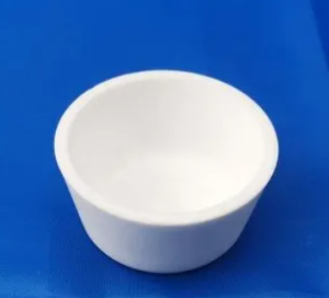
Unlike conventional graphite or quartz crucibles, silicon carbide crucibles are engineered to withstand the extreme conditions required to grow ultra-pure SiC crystals. This article dives into how this niche ceramic component is enabling breakthroughs in semiconductor manufacturing, far beyond kitchenware or industrial abrasives.
2. Why Silicon Carbide Crucibles? The Physics of Crystal Growth
Growing a single crystal of silicon carbide isn’t like melting sugar—it requires temperatures above 2,200°C in a near-vacuum environment. At these extremes, most materials degrade, react, or contaminate the melt. Enter the silicon carbide crucible.
Made from high-purity silicon carbide ceramic, these crucibles offer exceptional thermal stability, low thermal expansion, and chemical inertness. Crucially, they minimize carbon and metallic impurities that could ruin the electrical properties of the resulting wafer.
3. The PVT Process: Where Crucibles Make or Break Yield
3.1. Physical Vapor Transport (PVT) Explained

The dominant method for producing SiC boules is Physical Vapor Transport. In this process, SiC powder is placed in a crucible inside a sealed furnace. As the powder sublimates at high heat, vapor migrates upward and re-crystallizes on a cooler seed crystal, slowly forming a monolithic ingot.
The crucible isn’t just a container—it’s an active participant. Its geometry, porosity, and surface chemistry directly influence vapor flow, nucleation, and defect formation.
3.2. Material Purity Matters
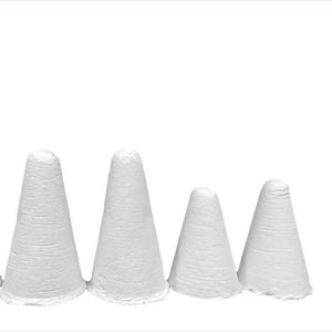
Even trace impurities from a crucible wall can introduce micropipes or dislocations in the crystal lattice. That’s why leading manufacturers use reaction-bonded silicon carbide (RBSiC) or sintered high-purity SiC—often custom-shaped as silicon carbide ceramic columns, rings, or tube assemblies—to line or construct the entire crucible system.
Interestingly, while silicon nitride crucible factory output is rising for other high-temp applications, SiC remains the gold standard for SiC crystal growth due to material compatibility. Boron carbide vs silicon carbide comparisons often favor SiC here for its superior thermal conductivity and lower reactivity with SiC vapor.
4. Beyond the Crucible: Supporting SiC Infrastructure

The crucible doesn’t operate in isolation. It’s part of a high-temperature ecosystem that includes:
- Silicon carbide thermocouple protection tubes for accurate temperature monitoring
- Silicon carbide ceramic tubes for furnace insulation and gas flow control
- Silicon carbide burner nozzles in pre-heating zones
- RBSiC silicon carbide tile blocks as structural supports
These components—often fabricated alongside crucibles—ensure thermal uniformity and mechanical integrity during weeks-long growth cycles.
5. Misconceptions: Kitchenware vs. Industrial Reality
A quick online search for ‘silicon carbide ceramic dish’ or ‘silicon carbide baking ceramic dish’ reveals a flood of cookware products. While these leverage SiC’s thermal shock resistance, they’re made from lower-purity, composite ceramics—nothing like the >99.9% pure, engineered crucibles used in semiconductor fabs.
Similarly, items like silicon carbide ceramic dinner plates, butter dishes, or Christmas platters are decorative or culinary novelties. They share a base material but serve entirely different purposes. Confusing them with industrial SiC components is like comparing a toy drone to a military UAV.
6. Future Outlook: Scaling Purity and Geometry
As 8-inch SiC wafers become standard, crucible design is evolving. Engineers now develop custom silicon carbide ring configurations and segmented crucibles to manage stress and improve yield. Some startups are even experimenting with silicon carbide porous ceramic tubes to fine-tune vapor pressure gradients.
Meanwhile, the high purity silicon nitride powder market is growing in parallel, supporting complementary components like custom silicon nitride heat shields and silicon nitride plates that protect furnace walls—but SiC remains irreplaceable at the core.
7. Conclusion
The silicon carbide crucible may never grace a dinner table, but it’s quietly enabling the electrified future. From EVs to 5G infrastructure, every SiC power device traces its origin to this unassuming ceramic vessel. As crystal growth techniques advance, so too will the precision engineering of SiC crucibles—proving that in high-tech manufacturing, even the container is mission-critical.
Our Website founded on October 17, 2012, is a high-tech enterprise committed to the research and development, production, processing, sales and technical services of ceramic relative materials such as Silicon. Our products includes but not limited to Boron Carbide Ceramic Products, Boron Nitride Ceramic Products, Silicon Carbide Ceramic Products, Silicon Nitride Ceramic Products, Zirconium Dioxide Ceramic Products, etc. If you are interested, please feel free to contact us.
RELATED POSTS
Differences and Applications Between Ceramic and Metal Crucibles
The Irreplaceability Of Alumina Ceramic Substrates In The Field Of Electronic Packaging
Removing Ceramic Tile Adhesive from Concrete Floors: Effective Methods

Why Are Silicon Nitride Ceramic Boards The Best Choice For High-End Electronic Equipment?
