Discover Premium Ceramic Products | Durability & Elegance United | Advanced Ceramics
1. Introduction
In a major development reported just 48 hours ago, Wolfspeed announced a $5 billion expansion of its silicon carbide wafer production facility in North Carolina, underscoring the surging global demand for SiC-based semiconductors in electric vehicles and renewable energy systems. Central to this manufacturing scale-up is a seemingly humble but indispensable component: the silicon carbide crucible.

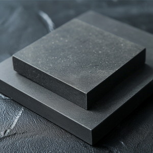
Silicon carbide crucibles are not your everyday labware. Engineered for extreme thermal stability and chemical inertness, they serve as the foundational vessel in the physical vapor transport (PVT) method—the dominant technique for growing high-quality silicon carbide single crystals. As the semiconductor industry races to meet the demands of next-generation power electronics, the performance of the silicon carbide crucible has become a bottleneck—and a strategic asset.
2. The Crucial Role of Silicon Carbide Crucibles in SiC Crystal Growth
2.1. Why Silicon Carbide?
Silicon carbide crucibles are uniquely suited for PVT crystal growth due to their exceptional properties. They withstand temperatures exceeding 2,200°C without deforming, resist thermal shock during rapid heating and cooling cycles, and exhibit minimal reactivity with molten or vapor-phase silicon and carbon.
Unlike graphite crucibles—which are commonly used but introduce carbon impurities—silicon carbide crucibles maintain the stoichiometry and purity of the growing crystal. This is vital for producing low-defect-density SiC wafers used in high-voltage, high-frequency applications.
2.2. Comparison with Alternative Ceramics
While silicon nitride crucible factory outputs have increased for other high-temperature applications, silicon nitride crucibles are generally unsuitable for SiC crystal growth due to potential nitrogen contamination and lower thermal conductivity at extreme temperatures.
Similarly, boron carbide vs silicon carbide comparisons show that boron carbide, though hard and refractory, lacks the thermal stability and oxidation resistance required in prolonged PVT runs. Thus, silicon carbide remains the material of choice.
3. Integration with Advanced Furnace Systems
Modern SiC crystal growth relies on sophisticated tube furnaces where the silicon carbide crucible is housed within a silicon carbide tube furnace assembly. These systems often incorporate silicon carbide ceramic tubes for furnace linings and silicon carbide thermocouple protection tubes to ensure accurate temperature monitoring.
Components like silicon carbide ceramic columns, silicon carbide ring spacers, and rbsic silicon carbide tile blocks are used to support and insulate the crucible, minimizing thermal gradients that could induce crystal defects.
4. Beyond Crucibles: The Broader Ecosystem of Silicon Carbide Components

The same material science that enables high-performance crucibles also drives innovation in related industrial ceramics. For instance, silicon carbide burner nozzles and silicon carbide brick linings are used in the same high-temperature furnaces to ensure uniform heating.
Meanwhile, silicon carbide discs—including silicon carbide ceramic grinding discs and silicon carbide diamond grinding discs for pottery—are employed in post-growth wafer slicing and polishing, linking crucible performance to final device yield.
5. Emerging Trends and Material Synergies
Although the focus here is on crucibles, it’s worth noting that silicon carbide’s versatility extends into consumer and industrial domains. Products like silicon carbide ceramic baking dishes, silicon carbide ceramic dinner plates, and even silicon carbide ceramic butter dishes leverage the material’s thermal shock resistance—though these use lower-purity grades than semiconductor applications.
Conversely, high-purity applications demand materials like high purity silicon nitride powder for custom silicon nitride heat shields or silicon nitride plates used in adjacent semiconductor processes, highlighting a complementary—but distinct—role for silicon nitride ceramics.
6. Challenges and Future Outlook
Despite their advantages, silicon carbide crucibles face challenges in cost and manufacturing complexity. Producing crack-free, high-density crucibles at scale requires advanced sintering techniques and stringent quality control.
However, with global investments in SiC wafer capacity accelerating—driven by EV makers like Tesla and infrastructure projects worldwide—the demand for reliable, high-performance silicon carbide crucibles is expected to grow exponentially over the next decade.
7. Conclusion
The silicon carbide crucible may be a small component in the vast semiconductor supply chain, but its role is pivotal. As the industry pushes the boundaries of power electronics, this niche ceramic vessel stands at the heart of innovation—enabling the growth of crystals that will power the clean energy transition. Its synergy with other silicon carbide components, from tubes to tiles, underscores the material’s unmatched versatility in extreme environments.
Our Website founded on October 17, 2012, is a high-tech enterprise committed to the research and development, production, processing, sales and technical services of ceramic relative materials such as Silicon. Our products includes but not limited to Boron Carbide Ceramic Products, Boron Nitride Ceramic Products, Silicon Carbide Ceramic Products, Silicon Nitride Ceramic Products, Zirconium Dioxide Ceramic Products, etc. If you are interested, please feel free to contact us.