Discover Premium Ceramic Products | Durability & Elegance United | Advanced Ceramics
1. Introduction
Just 24 hours ago, leading semiconductor manufacturer GlobalWafers announced a breakthrough in 300mm silicon ingot production using next-generation crystal pullers equipped with high-purity silicon carbide crucibles. This development underscores a growing industry shift toward silicon carbide (SiC) components in ultra-high-temperature, contamination-sensitive processes. While many associate silicon carbide with ceramic dinnerware or brake discs, its most transformative applications lie in advanced materials engineering—particularly in the controlled growth of single-crystal silicon for chips that power everything from smartphones to electric vehicles.

Silicon carbide crucibles are not your average labware. Engineered for extreme environments, they withstand temperatures exceeding 1,600°C while resisting chemical attack from molten silicon—a feat few ceramics can match. This article dives into why silicon carbide crucibles have become indispensable in semiconductor crystal growth, how they compare to alternatives like silicon nitride or boron carbide, and why their industrial role is often confused with unrelated consumer products like silicon carbide ceramic baking dishes.
2. The Crucial Role of Silicon Carbide Crucibles in Czochralski Crystal Growth
The Czochralski (CZ) method remains the dominant technique for producing monocrystalline silicon ingots used in integrated circuits. In this process, polycrystalline silicon is melted in a crucible, and a seed crystal is slowly pulled upward while rotating, forming a large, defect-free single crystal. The crucible must endure prolonged exposure to molten silicon at ~1,420°C without contaminating the melt or deforming under thermal stress.
Traditional quartz crucibles degrade over time, releasing oxygen into the silicon melt and creating defects that reduce chip yield. Silicon carbide crucibles, by contrast, offer exceptional thermal conductivity, low thermal expansion, and remarkable chemical inertness. High-purity reaction-bonded silicon carbide (RBSiC) crucibles—often fabricated as rbsic silicon carbide tile blocks or custom-molded vessels—minimize impurity diffusion and maintain structural integrity over hundreds of growth cycles.

3. Silicon Carbide vs. Alternatives: Why Not Silicon Nitride or Boron Carbide?
When engineers evaluate high-temperature crucible materials, silicon nitride and boron carbide often enter the conversation. Silicon nitride crucible factories produce components with excellent thermal shock resistance, but silicon nitride reacts with molten silicon above 1,400°C, forming silicides that compromise purity. Similarly, while boron carbide is extremely hard, it introduces boron dopants into the melt—unacceptable in semiconductor-grade silicon where dopant concentrations must be precisely controlled.
This is where boron carbide vs silicon carbide comparisons fall short in semiconductor contexts: silicon carbide’s compatibility with molten silicon is unmatched. Moreover, silicon carbide ceramic columns, rings, and burner nozzles used in ancillary furnace components benefit from the same material advantages—making SiC a holistic solution for high-temperature semiconductor infrastructure.
4. Debunking the Dinnerware Confusion
A quick online search for ‘silicon carbide ceramic dish’ yields hundreds of results for baking pans, butter dishes, and even Christmas plates. While these products may contain trace silicon carbide for thermal shock resistance, they are fundamentally different from industrial-grade silicon carbide crucibles. Consumer items like silicon carbide ceramic dinner plates or casserole dishes are typically porcelain or stoneware with SiC additives—not monolithic, high-purity SiC ceramics.
True silicon carbide crucibles are manufactured through sintering or reaction bonding of high purity silicon nitride powder market-grade precursors, yielding dense, non-porous structures. In contrast, a silicon carbide baking ceramic dish from a kitchenware brand like Staub uses SiC merely as a filler. Confusing these applications leads to unrealistic expectations about performance—and highlights why industrial SiC components require specialized fabrication, not artisanal glazing.
5. Beyond Crucibles: Supporting Infrastructure in Semiconductor Furnaces
The utility of silicon carbide extends beyond the crucible itself. Furnace linings often incorporate silicon carbide brick or porous ceramic tubes for insulation and gas flow control. Silicon carbide thermocouple protection tubes shield temperature sensors from corrosive atmospheres, while silicon carbide ceramic tube insulators maintain electrical isolation in heating elements.
Even ancillary parts like silicon carbide disc taps or ceramic grinding discs used in maintenance rely on SiC’s hardness and wear resistance. However, these are distinct from the ultra-high-purity demands of crystal growth. The key differentiator is material grade: semiconductor applications require parts fabricated from electronic-grade SiC with impurity levels below 1 ppm—far beyond what’s needed for plumbing pipes or sanding discs.
6. Conclusion
Silicon carbide crucibles are a linchpin in modern semiconductor manufacturing, enabling the production of ultra-pure silicon crystals that drive technological progress. Their superiority over alternatives like silicon nitride or boron carbide in high-temperature, contamination-sensitive environments is well-established. While the term ‘silicon carbide’ appears in everything from ceramic salad bowls to industrial burner nozzles, the performance requirements—and material science—behind a semiconductor crucible are in a league of their own. As chipmakers push toward larger wafers and tighter defect tolerances, the demand for advanced silicon carbide components will only grow.
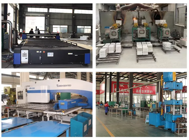
Our Website founded on October 17, 2012, is a high-tech enterprise committed to the research and development, production, processing, sales and technical services of ceramic relative materials such as Why. Our products includes but not limited to Boron Carbide Ceramic Products, Boron Nitride Ceramic Products, Silicon Carbide Ceramic Products, Silicon Nitride Ceramic Products, Zirconium Dioxide Ceramic Products, etc. If you are interested, please feel free to contact us.