Discover Premium Ceramic Products | Durability & Elegance United | Advanced Ceramics
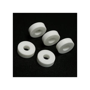
PRODUCT PARAMETERS
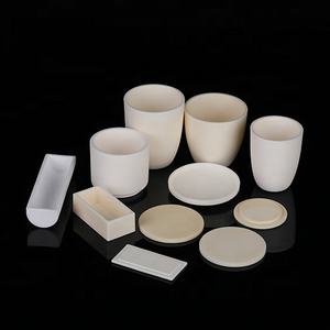
Description
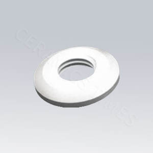
Overview of Boron Nitride Bn Ceramics for Semiconductor
Boron Nitride (BN) ceramic is a unique material renowned for its exceptional properties, making it highly valuable in various industrial applications. It exists in multiple forms, primarily hexagonal boron nitride (h-BN), cubic boron nitride (c-BN), and wurtzite boron nitride (w-BN). Hexagonal BN, the most common form, is often compared to graphite due to its lubricious and thermally conductive yet electrically insulating nature. Boron Nitride ceramics are synthesized under high temperatures and pressures, offering a rare combination of properties not found in many other materials.
Features of Boron Nitride Bn Ceramics for Semiconductor
Thermal Conductivity: Excellent thermal conductivity, especially in the hexagonal form, allowing efficient heat dissipation.
Electrical Insulation: Outstanding electrical insulation properties make it ideal for electrical applications requiring thermal management.
Chemical Stability: Highly resistant to chemical attacks, including strong acids and bases, ensuring durability in harsh environments.
Thermal Shock Resistance: Superior resistance to thermal shock, enabling it to withstand rapid temperature changes without cracking.
Mechanical Strength: Good mechanical strength at both room and elevated temperatures, although this can vary with the form of BN.
Lubricity: Self-lubricating property due to its layered structure, which reduces friction and wear in moving parts.
Non-Toxic: Safe to use in various settings, including medical and food processing industries, due to its non-toxic nature.
High-Temperature Performance: Maintains stability at extremely high temperatures, exceeding 1000°C in inert atmospheres, making it suitable for refractory applications.
(Boron Nitride Bn Ceramics for Semiconductor)
Specification of Boron Nitride Bn Ceramics for Semiconductor
Boron nitride ceramics are advanced materials. They are vital in semiconductor manufacturing. BN ceramics offer unique properties. They handle extreme heat well. Their thermal conductivity is high. It matches some metals. Heat moves through them quickly. This prevents overheating in devices. BN ceramics are strong electrical insulators. They block electricity completely. This is critical near electronic parts. They stop unwanted currents. They resist very high voltages. BN ceramics are chemically stable. They do not react with most chemicals. Common acids and bases do not harm them. Molten metals do not stick to them. This ensures long life in harsh processes. They handle sudden temperature changes. They do not crack under thermal shock. This is important for rapid heating or cooling steps. BN ceramics are easy to machine. They can be cut and shaped precisely. This allows custom parts for specific tools. Their surface is very smooth. This minimizes particle generation. Cleanliness is essential in semiconductor fabs. BN ceramics are lightweight. They are much lighter than metals like steel. This helps in handling delicate wafers. They are non-toxic and safe to use. Their low thermal expansion is key. They keep their shape when heated. This prevents warping near hot zones. They provide excellent electrical isolation. Heat sinks often use them. They sit between hot components and coolers. Their stability prevents contamination. They maintain purity in the process chamber. They are reliable under vacuum. They work well in CVD and PVD systems. They support wafers during high-temperature steps. Their combination of properties is rare. Few materials match BN for these tasks. They machine precisely. They meet tight tolerances needed for semiconductor equipment.
(Boron Nitride Bn Ceramics for Semiconductor)
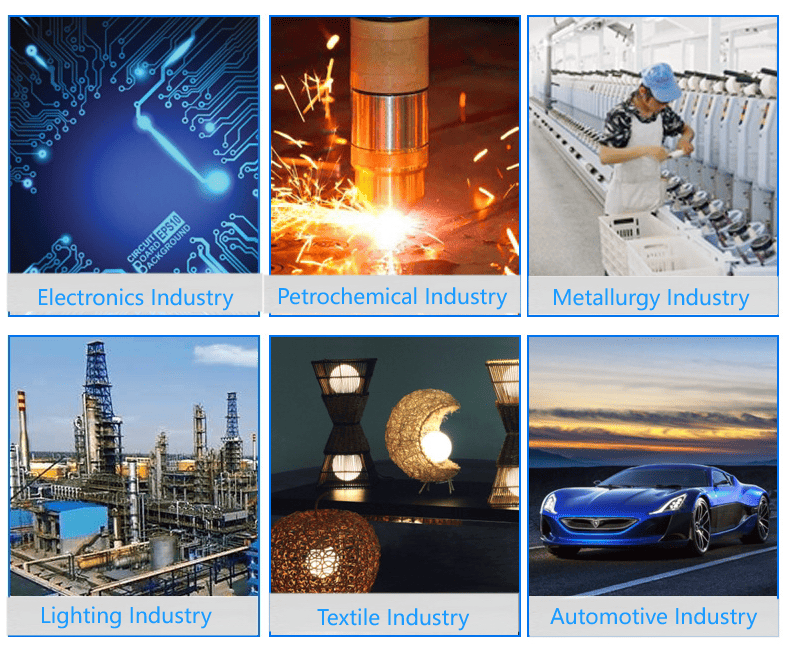
Applications of Boron Nitride Bn Ceramics for Semiconductor
Boron nitride ceramics do important jobs in semiconductor manufacturing. They handle extreme conditions well. Semiconductor processes need this. BN ceramics work perfectly here.
One big use is for crucibles. These hold molten materials. Making silicon chips starts with melting stuff. BN crucibles resist the heat. They also keep the material pure. Contamination ruins semiconductors. BN stays clean. It doesn’t react. This purity is critical.
Another key job is insulation parts. Semiconductor equipment gets very hot. Plasma etching and other processes run hot. BN insulates extremely well. It stops heat where it shouldn’t go. Equipment parts stay safe. BN also resists plasma damage. Plasma doesn’t easily wear it down. Parts last longer. Production keeps running smoothly.
Heat spreading is vital too. Small chips generate lots of heat. This heat must go away fast. BN helps move heat quickly. It conducts heat better than alumina. BN parts sit near the hot chip. They pull the heat out efficiently. The chip stays cooler. Performance stays high. Reliability improves.
BN also matches silicon well. Silicon expands when hot. BN expands similarly. This means less stress. BN parts holding silicon wafers don’t crack them. Temperature changes happen safely. Wafer breakage drops. Yield goes up. This dimensional stability is a major advantage.
Handling wafers needs care. BN makes good fixtures. It grips wafers without scratching. The surface stays perfect. BN is also electrically insulating. No unwanted currents flow. This protects delicate circuits.
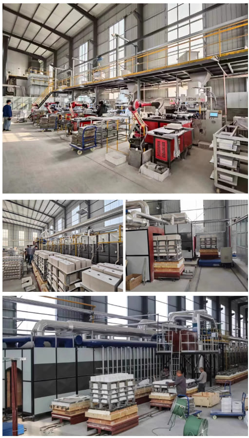
Company Introduction
Advanced Ceramics founded on October 17, 2014, is a high-tech enterprise committed to the research and development, production, processing, sales and technical services of ceramic relative materials and products.. Since its establishment in 2014, the company has been committed to providing customers with the best products and services, and has become a leader in the industry through continuous technological innovation and strict quality management.
Our products includes but not limited to Silicon carbide ceramic products, Boron Carbide Ceramic Products, Boron Nitride Ceramic Products, Silicon Carbide Ceramic Products, Silicon Nitride Ceramic Products, Zirconium Dioxide Ceramic Products, Quartz Products, etc. Please feel free to contact us.
Payment Methods
T/T, Western Union, Paypal, Credit Card etc.
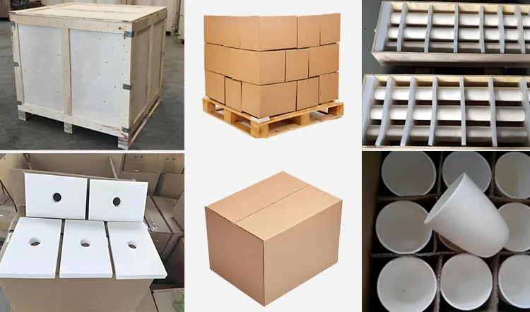
Shipment Methods
By air, by sea, by express, as customers request.
5 FAQs of Boron Nitride Bn Ceramics for Semiconductor
What is boron nitride ceramic good for in semiconductors?
Boron nitride ceramic handles extreme heat well. It moves heat away from sensitive parts fast. This prevents overheating. It also doesn’t conduct electricity. This keeps parts safe from electrical shorts. Many semiconductor tools use it.
Why pick boron nitride over aluminum nitride?
Boron nitride handles sudden temperature changes better. It won’t crack easily from heat shock. It’s also softer. This makes it easier to machine into exact shapes. Its electrical insulation works better at high heat. Aluminum nitride conducts electricity slightly when very hot.
Can boron nitride ceramics touch silicon wafers?
Yes, it’s safe. Boron nitride doesn’t contaminate silicon. It won’t release harmful particles. Its surface is smooth. Wafers won’t get scratched. This makes it reliable for holding wafers during high-heat processes.
Is boron nitride ceramic expensive?
Yes, it costs more than many other ceramics. Making it needs special processes. This increases the price. But its performance is unique. The extra cost is often worth it. It helps tools last longer and work better.
How long does boron nitride ceramic last?
It lasts a long time under normal use. It resists wear well. It doesn’t react with most chemicals. High heat doesn’t damage it. Regular cleaning is needed. Avoid strong impacts. Handled right, it provides years of service.
(Boron Nitride Bn Ceramics for Semiconductor)
REQUEST A QUOTE
RELATED PRODUCTS
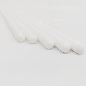
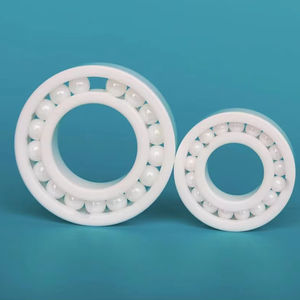
China High Thermal Conductivity Boron Nitride Ceramic Parts
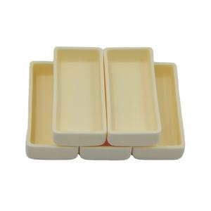
Industry Ceramic High Temprature Resistant Boron Nitride Products
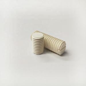
Industry Ceramic Heat Resistant Boron Nitride Parts
High Temperature Nano Hexagonal Boron Nitride Powder 200-500nm HBN Boron Nitride for Coating Ceramic Cosmetic
High-Temperature Boron Nitride Ceramic Structure Ceramic