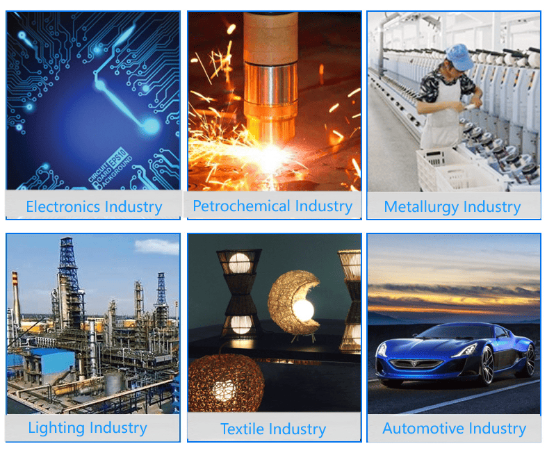
Discover Premium Ceramic Products | Durability & Elegance United | Advanced Ceramics
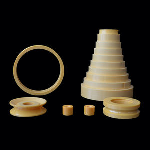
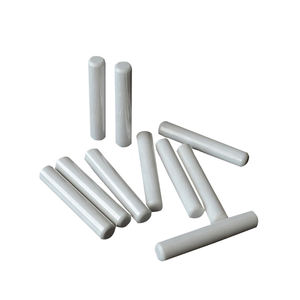
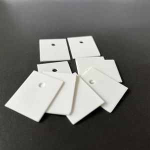
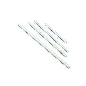
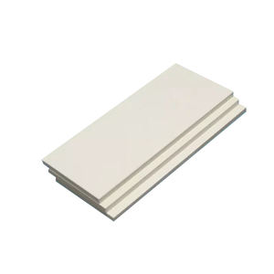
PRODUCT PARAMETERS
Description
Overview of High Purity Bn Boron Nitride Ceramic Block for Semiconductor Industry
Boron Nitride (BN) ceramic is a unique material renowned for its exceptional properties, making it highly valuable in various industrial applications. It exists in multiple forms, primarily hexagonal boron nitride (h-BN), cubic boron nitride (c-BN), and wurtzite boron nitride (w-BN). Hexagonal BN, the most common form, is often compared to graphite due to its lubricious and thermally conductive yet electrically insulating nature. Boron Nitride ceramics are synthesized under high temperatures and pressures, offering a rare combination of properties not found in many other materials.
Features of High Purity Bn Boron Nitride Ceramic Block for Semiconductor Industry
Thermal Conductivity: Excellent thermal conductivity, especially in the hexagonal form, allowing efficient heat dissipation.
Electrical Insulation: Outstanding electrical insulation properties make it ideal for electrical applications requiring thermal management.
Chemical Stability: Highly resistant to chemical attacks, including strong acids and bases, ensuring durability in harsh environments.
Thermal Shock Resistance: Superior resistance to thermal shock, enabling it to withstand rapid temperature changes without cracking.
Mechanical Strength: Good mechanical strength at both room and elevated temperatures, although this can vary with the form of BN.
Lubricity: Self-lubricating property due to its layered structure, which reduces friction and wear in moving parts.
Non-Toxic: Safe to use in various settings, including medical and food processing industries, due to its non-toxic nature.
High-Temperature Performance: Maintains stability at extremely high temperatures, exceeding 1000°C in inert atmospheres, making it suitable for refractory applications.
(High Purity Bn Boron Nitride Ceramic Block for Semiconductor Industry)
Specification of High Purity Bn Boron Nitride Ceramic Block for Semiconductor Industry
High pureness BN boron nitride ceramic blocks offer critical functions in semiconductor manufacturing. These blocks provide outstanding thermal stability and electrical insulation. They withstand severe temperature levels beyond 2000 ° C. This makes them ideal for demanding processes. Semiconductor devices like CVD chambers and epitaxy systems rely upon them.
Purity is extremely important. Our BN obstructs attain purity levels surpassing 99.99%. This minimizes contamination dangers for sensitive wafers. Trace steel impurities are purely regulated, typically below 10ppm. Reduced oxygen and carbon material are likewise ensured. High pureness ensures consistent process outcomes and secures pricey semiconductor materials.
Thermal performance is superior. BN ceramic has extremely reduced thermal growth. This prevents cracking under fast temperature level changes. Its thermal conductivity is moderate. Warmth spreads evenly, avoiding hotspots. The product is also an excellent electric insulator. This protects against undesirable currents in processing devices.
Mechanical buildings are strong. BN ceramic is tough and wear-resistant. It deals with physical tension well. The product is also conveniently machinable. Exact forms and smooth surface areas are attainable. Surface area finish is important. Great surfaces avoid fragment generation inside tidy devices.
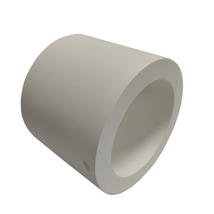
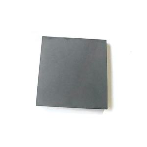
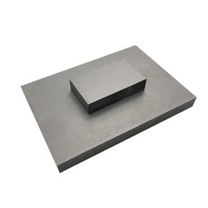
Common sizes are available. Usual measurements include 100x100x10mm or 200x200x20mm. Custom-made dimensions are feasible. We maker obstructs to exact customer drawings. Tight tolerances are maintained for perfect fit. These blocks are made use of in diffusion heaters, MOCVD activators, and various other high-temperature semiconductor tools. They function as crucibles, heaters, insulators, and safety plates. Reputable performance is vital for high-yield semiconductor manufacturing.
(High Purity Bn Boron Nitride Ceramic Block for Semiconductor Industry)
Applications of High Purity Bn Boron Nitride Ceramic Block for Semiconductor Industry
High pureness BN boron nitride ceramic blocks are essential in semiconductor manufacturing. They use one-of-a-kind homes essential for sophisticated chip production. This product withstands incredibly high temperatures conveniently. It remains stable beyond 2000 ° C. Thermal shock resistance is outstanding. Blocks heat up or cool off quick without breaking. This is important for quick thermal processing actions.
Electrical insulation is one more significant benefit. BN blocks are superb insulators even at high warmth. They stop undesirable electric currents in devices. Chemical inertness is key. High purity BN does not respond with molten silicon, gallium arsenide, or procedure gases. It keeps the production atmosphere tidy. Contamination dangers are really reduced. This shields delicate wafers and enhances chip yields.
Semiconductor makers make use of these ceramic blocks in details ways. They are perfect crucibles for melting and taking shape silicon. BN crucibles support growing large, pure ingots. The blocks work as insulating plates and guards inside crystal pullers. They take care of warm effectively around the warm zone. In wafer handling, BN makes resilient trays and carriers. These safely move wafers through high-temperature heating systems without damages.
Plasma etching and deposition tools rely upon BN elements too. The ceramic serve as guards, nozzles, and linings. It stands up to hostile plasma chemistries. Its electric insulation stops arcing troubles. Precision machining permits tight dimensional control. BN parts fit perfectly right into complicated semiconductor devices. This makes sure regular procedure results chip makers require.
Company Introduction
Advanced Ceramics founded on October 17, 2014, is a high-tech enterprise committed to the research and development, production, processing, sales and technical services of ceramic relative materials and products.. Since its establishment in 2014, the company has been committed to providing customers with the best products and services, and has become a leader in the industry through continuous technological innovation and strict quality management.
Our products includes but not limited to Silicon carbide ceramic products, Boron Carbide Ceramic Products, Boron Nitride Ceramic Products, Silicon Carbide Ceramic Products, Silicon Nitride Ceramic Products, Zirconium Dioxide Ceramic Products, Quartz Products, etc. Please feel free to contact us.
Payment Methods
T/T, Western Union, Paypal, Credit Card etc.
Shipment Methods
By air, by sea, by express, as customers request.
5 FAQs of High Purity Bn Boron Nitride Ceramic Block for Semiconductor Industry
High Purity BN Boron Nitride Ceramic Block: Top 5 FAQs for Semiconductors
What makes high purity BN ceramic blocks special for semiconductors?
Ultra-high purity is essential. Impurities ruin sensitive semiconductor processes. Our BN blocks exceed 99.99% purity. This minimizes contamination risks on silicon wafers. Clean wafers mean better chip yields.
What are the key properties of BN blocks for our industry?
BN offers excellent thermal stability. It handles extreme heat in CVD chambers easily. BN is also chemically inert. It resists attack from harsh process gases and molten metals. Electrical insulation is another critical feature. BN prevents unwanted currents near wafers.
Where are these BN blocks used in semiconductor tools?
They are vital components inside high-temperature equipment. You find them in MOCVD and MBE systems. BN blocks act as crucibles, heaters, insulators, and shields. Their job is protecting wafers and maintaining process integrity under tough conditions.
How do we handle and maintain BN ceramic blocks?
Handle BN blocks carefully. Avoid impacts. Chipping can create particles. Clean blocks only with approved methods. Never use abrasive materials. Follow the manufacturer’s cleaning protocol strictly. Proper handling extends block life and prevents tool contamination.
Why choose BN over other ceramics for these applications?
Other ceramics like alumina often release trace metals at high temperatures. BN does not. Its thermal shock resistance is superior. BN blocks survive rapid heating and cooling cycles without cracking. This reliability reduces downtime. BN’s unique combination of purity, stability, and performance is unmatched for critical semiconductor processes.
(High Purity Bn Boron Nitride Ceramic Block for Semiconductor Industry)
REQUEST A QUOTE
RELATED PRODUCTS
boron nitride ceramic Pyrolytic boron nitride crucible HBN ceramic crucible boron nitride tube
Electric Conduction BN Boron Nitride Composite Ceramic Crucibles Evaporative Silicon And Aluminum Plating
99% 50-100 um Aggregates BN Powder Ceramic Hexagonal Boron Nitride Powder
High Purity BN Insulating Ceramic Plate Boron Nitride Sheet Structural Parts
Hot Preesing Boron Nitride Ceramic Insulating Parts Electrode Protection