Discover Premium Ceramic Products | Durability & Elegance United | Advanced Ceramics
PRODUCT PARAMETERS
Description
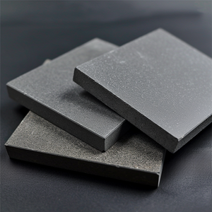
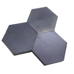
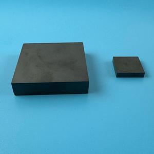
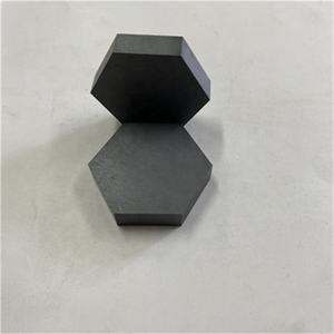
Overview of High Hardness Silicon Carbide Sic Ceramic Wafer in Semiconductor Industry
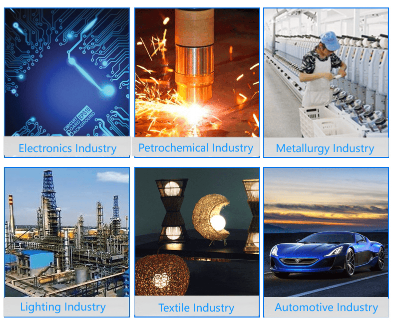
Silicon Carbide (SiC) ceramics are renowned for their outstanding mechanical properties, including high hardness, strength at elevated temperatures, and excellent thermal shock resistance. These materials are pivotal in cutting-edge industrial applications, from abrasives to aerospace components, due to their unique combination of properties.
Features of High Hardness Silicon Carbide Sic Ceramic Wafer in Semiconductor Industry
High Hardness: Exceptional wear resistance.
Thermal Shock Resistance: Can withstand rapid temperature changes.
Chemical Stability: Resistant to most chemicals.
High Thermal Conductivity: Efficient heat dissipation.
Low Density: Lightweight for its strength.
(High Hardness Silicon Carbide Sic Ceramic Wafer in Semiconductor Industry)
Specification of High Hardness Silicon Carbide Sic Ceramic Wafer in Semiconductor Industry
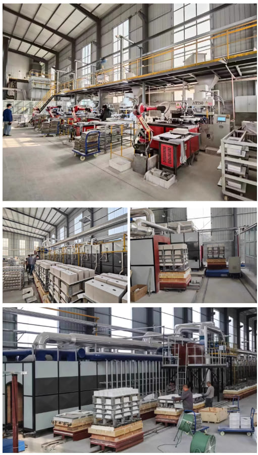
High firmness silicon carbide ceramic wafers are vital in sophisticated semiconductor manufacturing. They offer one-of-a-kind homes silicon wafers can not match. These SiC wafers are extremely hard. They stand up to scraping and use much better than silicon. This hardness is crucial for managing requiring processes. Semiconductor fabrication involves severe chemicals and physical tension. SiC wafers endure this atmosphere reliably. Their sturdiness means less replacements and less downtime.
Thermal management is an additional significant advantage. SiC performs warm remarkably well. Tools generate substantial heat throughout procedure. Effective warmth elimination is vital. SiC wafers pull heat far from sensitive components efficiently. This stops overheating and improves gadget performance. Power electronics profit significantly from this. These devices run at high temperatures usually. SiC wafers take care of the heat, boosting stability and life-span.
Electrical insulation is a crucial feature as well. SiC is a superb electrical insulator. It avoids undesirable present flow between layers. This isolation is essential for intricate circuit styles. It guarantees signals travel appropriately without disturbance. Gadget integrity raises dramatically. Producers depend on SiC wafers for high-power, high-frequency applications. Electric vehicles and renewable resource systems depend on them. Radar and interaction devices also utilize SiC substrates.
The pureness and surface high quality of these wafers are tightly managed. Any defect can mess up a semiconductor device. Production follows strict standards. This guarantees regular performance batch after set. SiC wafers sustain smaller, much more effective electronics. They allow modern technologies needing remarkable thermal and electric control. Using them causes extra effective, sturdy semiconductor items.
(High Hardness Silicon Carbide Sic Ceramic Wafer in Semiconductor Industry)
Applications of High Hardness Silicon Carbide Sic Ceramic Wafer in Semiconductor Industry
High firmness silicon carbide ceramic wafers are essential in contemporary semiconductors. SiC wafers are extremely challenging. This hardness matters. It suggests they withstand damage throughout handling. They handle rough conditions well. SiC likewise holds up against severe warm. Typical silicon wafers fail at high temperatures. SiC wafers keep working. This warm resistance is critical.
Warm relocations well through SiC. This home is thermal conductivity. Excellent warmth circulation stops getting too hot. Instruments remain cooler. They carry out much better. Integrity raises significantly. Power electronics benefit greatly. SiC wafers are the base for effective chips. These chips regulate electricity efficiently. Less power gets thrown away as warm.
Electric cars and trucks use SiC power tools. The gadgets take care of battery power. They control the electric motor. SiC chips make systems smaller sized. They make battery chargers much faster. Energy savings are significant. Power grids additionally make use of SiC innovation. It assists manage power circulation better. Renewable resource systems count on SiC. Solar inverters function much more successfully. Wind power converters enhance.
Production requires solid products. SiC wafers fulfill this requirement. They sustain harsh manufacture actions. Etching and polishing are extreme procedures. SiC survives without warping. Wafer shape stays specific. This precision is essential. It guarantees layers build appropriately. Tool yields stay high. Manufacturing prices get controlled. SiC allows next-generation power tools. These gadgets push performance limits. They operate popular environments. Aerospace and defense applications utilize them. Industrial drives need their toughness. The semiconductor market maintains advancing. High firmness SiC wafers are essential. They make effective, effective electronics feasible.
Company Introduction
Advanced Ceramics founded on October 17, 2014, is a high-tech enterprise committed to the research and development, production, processing, sales and technical services of ceramic relative materials and products.. Since its establishment in 2014, the company has been committed to providing customers with the best products and services, and has become a leader in the industry through continuous technological innovation and strict quality management.
Our products includes but not limited to Silicon carbide ceramic products, Boron Carbide Ceramic Products, Boron Nitride Ceramic Products, Silicon Carbide Ceramic Products, Silicon Nitride Ceramic Products, Zirconium Dioxide Ceramic Products, Quartz Products, etc. Please feel free to contact us.
Payment Methods
T/T, Western Union, Paypal, Credit Card etc.
Shipment Methods
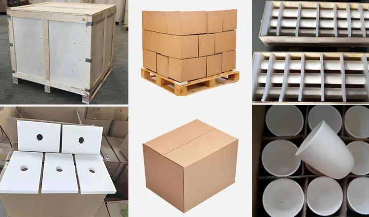
By air, by sea, by express, as customers request.
5 FAQs of High Hardness Silicon Carbide Sic Ceramic Wafer in Semiconductor Industry
Silicon carbide ceramic wafers are important in semiconductors. Here are five common questions about them.
What is a silicon carbide ceramic wafer?
It is a thin slice made from silicon carbide. This material is very hard. It handles high heat and electricity well. Factories use it for making powerful electronic parts.
Why use silicon carbide in semiconductors?
Silicon carbide beats normal silicon in key ways. It works at higher temperatures. It handles higher voltages. It switches power faster. This makes devices smaller and more efficient.
What benefits do silicon carbide wafers offer?
They last longer under stress. They waste less power as heat. They let devices run hotter safely. This means better performance in things like electric cars or power supplies.
Are there problems with silicon carbide wafers?
Yes. They cost more to make than silicon wafers. They are harder to cut and polish. Small defects can happen during production. These steps need special tools and care.
How are these wafers produced?
Raw silicon carbide powder gets pressed and heated. This forms a solid block. Then it is sliced into thin wafers. Each wafer is ground flat and polished. Finally, it is cleaned for use in chip making.
(High Hardness Silicon Carbide Sic Ceramic Wafer in Semiconductor Industry)
REQUEST A QUOTE
RELATED PRODUCTS
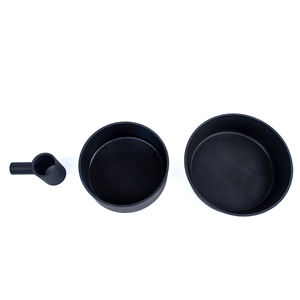
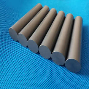
Custom Processing SIC Silicon Carbide Ceramic Strip Article for Industry Ceramic Parts SISIC Rods
Customized High Quality Silicon Carbide Ceramic Nozzle Black Sic Ceramic Rod/Tube/Parts

125mm 100mm Grinder Ceramic Zirconium Aluminum Oxide Silicon Carbide Fibre Discs Paper
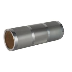
Recrystallized Silicon Carbide Beam Ssic Roller for Ceramic Industry
High Quality Refractory Silicon Carbide Sic Carbide Ceramic Plate Sinter Reaction Plate