Discover Premium Ceramic Products | Durability & Elegance United | Advanced Ceramics
PRODUCT PARAMETERS
Description
Overview of Silicon Carbide Ceramics
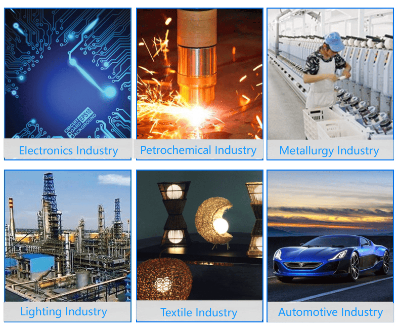
Silicon Carbide (SiC) ceramics are renowned for their outstanding mechanical properties, including high hardness, strength at elevated temperatures, and excellent thermal shock resistance. These materials are pivotal in cutting-edge industrial applications, from abrasives to aerospace components, due to their unique combination of properties.
Features of Silicon Carbide Ceramics
High Hardness: Exceptional wear resistance.
Thermal Shock Resistance: Can withstand rapid temperature changes.
Chemical Stability: Resistant to most chemicals.
High Thermal Conductivity: Efficient heat dissipation.
Low Density: Lightweight for its strength.
(Silicon Carbide SiC Porous Ceramic Plate for Semiconductor Industry)
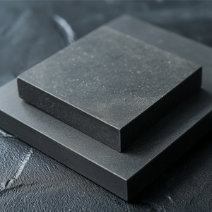
Specification of Silicon Carbide SiC Porous Ceramic Plate for Semiconductor Industry
The Silicon Carbide (SiC) Porous Porcelain Plate is made for high-performance applications in the semiconductor industry. This item utilizes premium silicon carbide product. It integrates high thermal conductivity with outstanding chemical resistance. The porous framework permits uniform gas or fluid circulation. This function is vital for procedures like wafer handling or chemical vapor deposition.
Home plate has a porosity range of 30-50%. Pore dimensions are adjustable between 5-200 microns. This makes sure specific control over fluid or gas flow. The product stands up to temperatures as much as 1600 ° C. It remains secure in quick thermal biking settings. This reduces breaking threats under severe heat. The ceramic plate stands up to rust from acids, antacid, and plasma. It performs dependably in aggressive semiconductor fabrication actions.
Mechanical toughness is a vital advantage. Home plate preserves structural integrity under high stress. It is suitable for load-bearing applications like wafer polishing. Surface area flatness is securely managed. Inconsistencies are kept below 0.05 mm throughout the entire plate. This avoids flaws throughout lithography or etching processes. Personalized shapes and sizes are available. Usual measurements include 200mm, 300mm, and 450mm diameters. Thickness arrays from 10mm to 50mm.
The product works with cleanroom criteria. It generates marginal fragments throughout use. This aligns with ISO Class 1-3 needs. Setup is uncomplicated. Home plate incorporates with existing semiconductor tools. Upkeep demands are reduced. Lengthy service life reduces substitute regularity.
Compared to conventional materials like alumina or quartz, SiC permeable ceramic offers premium thermal monitoring. It eliminates hotspots in high-power tools. Power efficiency boosts during processes like epitaxy. Prices connected to downtime decrease. Manufacturing returns increase due to constant efficiency.
Applications include wafer carriers, diffusion plates, and susceptors. The plate is used in CVD, etching, and annealing systems. It sustains innovative semiconductor production for gadgets like power electronics and LEDs. Personalized porosity and permeability choices are offered. These fulfill certain process requirements.
(Silicon Carbide SiC Porous Ceramic Plate for Semiconductor Industry)
Applications of Silicon Carbide SiC Porous Ceramic Plate for Semiconductor Industry
Silicon carbide (SiC) porous ceramic plates play a vital function in the semiconductor sector. These plates deal with extreme problems usual in semiconductor production. Their high thermal conductivity allows efficient warm dissipation during procedures like chemical vapor deposition. This prevents overheating in equipment. The permeable framework of SiC porcelains allows consistent gas circulation. This guarantees constant responses across semiconductor wafers.
SiC plates resist chemical deterioration from aggressive gases and acids. This durability prolongs their life expectancy in harsh settings. They preserve architectural integrity at temperature levels surpassing 1,600 ° C. This makes them suitable for high-temperature applications like wafer annealing.
The plates also function as filters for removing contaminations from process gases. Pollutants can harm semiconductor components. SiC’s fine pores trap bits without restricting gas flow. This improves item yield and decreases issues.
SiC permeable ceramics support wafer polishing. Their hardness minimizes wear throughout mechanical procedures. Surface area flatness is crucial for integrated circuit performance. These plates give secure, abrasion-resistant surface areas for precision sprucing up.
Semiconductor fabrication needs rigorous control of thermal expansion. SiC ceramics have reduced thermal development coefficients. This protects against warping or splitting under rapid temperature modifications. Refine security is kept.
Energy efficiency is an additional benefit. SiC’s thermal homes minimize the demand for energetic air conditioning systems. This decreases power usage in making centers.
Cost-effectiveness matters in high-volume manufacturing. SiC plates need much less regular substitute compared to typical products. Downtime is lessened. Production routines remain on track.
These plates adjust to sophisticated semiconductor innovations. They meet needs for smaller sized, faster chips. Their integrity supports next-generation devices like power electronic devices and 5G components.
SiC porous ceramic plates attend to multiple difficulties in semiconductor production. They incorporate thermal monitoring, chemical resistance, and mechanical toughness. Performance and efficiency enhance throughout production stages.
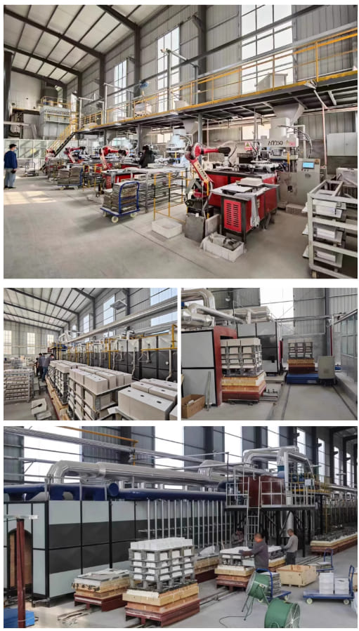
Company Introduction
Advanced Ceramics founded on October 17, 2014, is a high-tech enterprise committed to the research and development, production, processing, sales and technical services of ceramic relative materials and products.. Since its establishment in 2014, the company has been committed to providing customers with the best products and services, and has become a leader in the industry through continuous technological innovation and strict quality management.
Our products includes but not limited to Silicon carbide ceramic products, Boron Carbide Ceramic Products, Boron Nitride Ceramic Products, Silicon Carbide Ceramic Products, Silicon Nitride Ceramic Products, Zirconium Dioxide Ceramic Products, Quartz Products, etc. Please feel free to contact us.(nanotrun@yahoo.com)
Payment Methods
T/T, Western Union, Paypal, Credit Card etc.
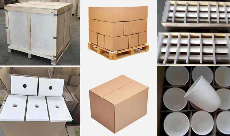
Shipment Methods
By air, by sea, by express, as customers request.
5 FAQs of Silicon Carbide SiC Porous Ceramic Plate for Semiconductor Industry
What is a Silicon Carbide Porous Ceramic Plate? Silicon Carbide (SiC) Porous Ceramic Plates are high-performance materials made by bonding silicon carbide grains to form a rigid structure with controlled porosity. These plates are used in semiconductor manufacturing for wafer handling, heat treatment, and processes requiring uniform gas or liquid distribution through their pores. The porous design allows precise flow control while maintaining strength and thermal stability.
Why are SiC plates preferred in the semiconductor industry? SiC plates offer exceptional heat resistance, chemical stability, and mechanical durability. They withstand extreme temperatures and corrosive environments common in semiconductor production. Their low thermal expansion reduces warping risks, ensuring consistent performance. The porous structure prevents contamination by minimizing particle generation, critical for maintaining cleanroom standards.
What temperature range can SiC porous plates handle? SiC porous plates operate reliably from room temperature up to 1600°C. They maintain structural integrity under rapid thermal cycling, making them ideal for processes like chemical vapor deposition (CVD) or annealing. Unlike metal or polymer alternatives, SiC does not degrade or release harmful byproducts at high temperatures.
How are SiC porous plates cleaned? Cleaning involves soaking or rinsing with acids, alkalis, or solvents to remove residues. The material’s chemical inertness ensures it resists damage from aggressive cleaning agents. Ultrasonic cleaning is also effective. Their non-porous surface layer prevents deep contamination, simplifying maintenance and extending service life.
Can SiC porous plates be customized? Yes. Manufacturers adjust pore size, shape, density, and plate dimensions to match specific applications. Customization ensures compatibility with equipment like wafer carriers or reaction chambers. Tailored porosity optimizes gas diffusion or filtration efficiency for different semiconductor processes. Testing validates performance before delivery.
(Silicon Carbide SiC Porous Ceramic Plate for Semiconductor Industry)
REQUEST A QUOTE
RELATED PRODUCTS
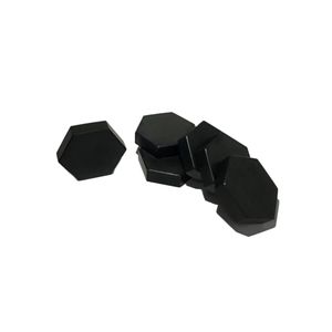
Pressureless Pressing Sintering SSiC Silicon Carbide Polished Ceramic Sheet Substrate Plate
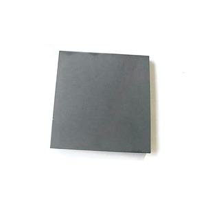
Factory Customized Silicon Carbided Sic Carbide Ceramic Plate Tiles Sheets Slabs Cutting Service Provided Welding Service
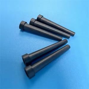
Silicon Carbide Ceramic Rod Ceramic Parts
1625C U W I Type Silicon Carbide Ceramic Heating Element Rods for Muffle Furnace
High Temperature/silicon Carbide Ceramic/SiC Ceramic Plate